- 您现在的位置:买卖IC网 > Sheet目录332 > IR21531STRPBF (International Rectifier)IC DRIVER HALF BRIDGE OSC 8SOIC
IR21531(D)(S) & (PbF)
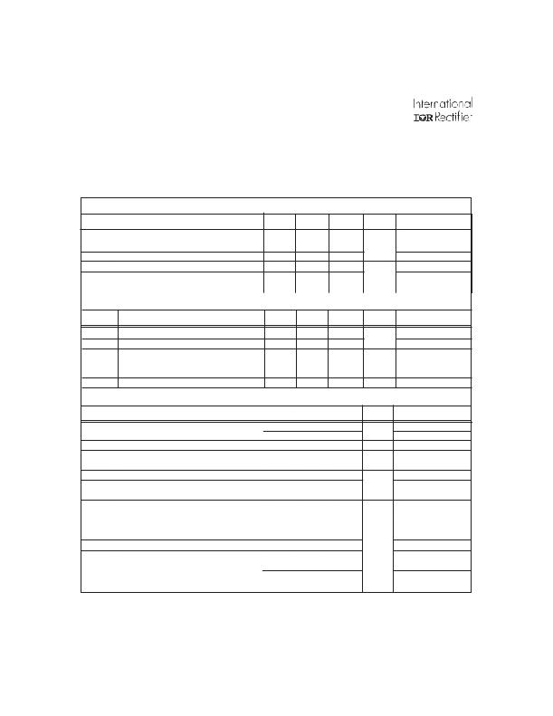
Electrical Characteristics
V BIAS (V CC , V BS ) = 12V, C L = 1000 pF, C T = 1 nF and T A = 25 ° C unless otherwise specified. The V IN , V TH and I IN
parameters are referenced to COM. The V O and I O parameters are referenced to COM and are applicable to the
respective output leads: HO or LO.
Low Voltage Supply Characteristics
Symbol Definition
Min.
Typ.
Max.
Units Test Conditions
V CCUV+
Rising V CC undervoltage lockout threshold
8.1
9.0
9.9
V CCUV-
V CCUVH
Falling V CC undervoltage lockout threshold
V CC undervoltage lockout Hysteresis
7.2
0.5
8.0
1.0
8.8
1.5
V
I QCCUV
I QCC
V CLAMP
Micropower startup V CC supply current
Quiescent V CC supply current
V CC zener clamp voltage
—
—
14.4
75
500
15.6
150
950
16.8
μ A
V
V CC ≤ V CCUV -
I CC = 5mA
Floating Supply Characteristics
Symbol Definition
Min.
Typ.
Max.
Units Test Conditions
I QBSUV
I QBS
V BSMIN
Micropower startup V BS supply current
Quiescent VBS supply current
Minimum required V BS voltage for proper
—
—
—
0
30
4.0
10
50
5.0
μ A
V
V CC ≤ V CCUV -
V CC =V CCUV+ + 0.1V
functionality from R T to HO
I LK
V F
Offset supply leakage current
Bootstrap diode forward voltage (IR21531D)
—
0.5
—
—
50
1.0
μ A
V
V B = V S = 600V
I F = 250mA
Oscillator I/O Characteristics
Symbol Definition
Min.
Typ.
Max.
Units
Test Conditions
fosc
d
I CT
I CTUV
V CT+
V CT-
V CTSD
V RT+
Oscillator frequency
R T pin duty cycle
C T pin current
UV-mode C T pin pulldown current
Upper C T ramp voltage threshold
Lower C T ramp voltage threshold
C T voltage shutdown threshold
High-level R T output voltage, V CC - V RT
19.4
94
48
—
0.30
—
—
1.8
—
20
100
50
0.001
0.70
8.0
4.0
2.1
10
20.6
106
52
1.0
1.2
—
—
2.4
50
kHz
%
uA
mA
V
R T = 36.9k ?
R T = 7.43k ?
fo < 100kHz
V CC = 7V
I RT = 100 μ A
—
100
300
I RT = 1mA
V RT-
Low-level R T output voltage
—
10
50
I RT = 100 μ A
V RTUV
V RTSD
UV-mode R T output voltage
SD-Mode R T output voltage, V CC - V RT
—
—
—
100
0
10
300
100
50
mV
I RT = 1mA
V CC ≤ V CCUV -
I RT = 100 μ A,
V CT = 0V
—
10
300
I RT = 1mA,
V CT = 0V
4
www.irf.com
发布紧急采购,3分钟左右您将得到回复。
相关PDF资料
IR2153DPBF
IC DVR HALF BRDG SELF-OSC 8-DIP
IR2155
IC DRVR HALF BRDG SELF-OSC 8-DIP
IR2181STRPBF
IC DRIVER HIGH/LOW SIDE 8SOIC
IR21834STRPBF
IC DRIVER HALF BRIDGE 14SOIC
IR21844SPBF
IC DRIVER HIGH/LOW SIDE 14SOIC
IR2213SPBF
IC DRIVER HIGH/LOW SIDE 16SOIC
IR22141SSPBF
IC DRIVER HALF BRIDGE SGL 24SSOP
IR2235JPBF
IC DRIVER BRIDGE 3PHASE 44PLCC
相关代理商/技术参数
IR21531STRPBF-CUT TAPE
制造商:IR 功能描述:IR2153 Series 600 V 200 mA 15.6 V Supply Dual Half Bridge Driver - SOIC-8
IR2153D
功能描述:IC HALF BRIDGE DRIVER W/DIO 8DIP RoHS:否 类别:集成电路 (IC) >> PMIC - MOSFET,电桥驱动器 - 外部开关 系列:- 标准包装:50 系列:- 配置:高端 输入类型:非反相 延迟时间:200ns 电流 - 峰:250mA 配置数:1 输出数:1 高端电压 - 最大(自引导启动):600V 电源电压:12 V ~ 20 V 工作温度:-40°C ~ 125°C 安装类型:通孔 封装/外壳:8-DIP(0.300",7.62mm) 供应商设备封装:8-DIP 包装:管件 其它名称:*IR2127
IR2153DPBF
功能描述:功率驱动器IC HALF BRDG DRVR 600V 210mA 1.2us RoHS:否 制造商:Micrel 产品:MOSFET Gate Drivers 类型:Low Cost High or Low Side MOSFET Driver 上升时间: 下降时间: 电源电压-最大:30 V 电源电压-最小:2.75 V 电源电流: 最大功率耗散: 最大工作温度:+ 85 C 安装风格:SMD/SMT 封装 / 箱体:SOIC-8 封装:Tube
IR2153DS
制造商:未知厂家 制造商全称:未知厂家 功能描述:Half Bridge Driver. LO In Phase with RT. Programmable Oscillating Frequency. 1.2us Deadtime in a 8-lead SOIC package with bootstrap diode
IR2153PBF
功能描述:功率驱动器IC HALF BRDG DRVR 600V 15.6Vclamp 1.2 RoHS:否 制造商:Micrel 产品:MOSFET Gate Drivers 类型:Low Cost High or Low Side MOSFET Driver 上升时间: 下降时间: 电源电压-最大:30 V 电源电压-最小:2.75 V 电源电流: 最大功率耗散: 最大工作温度:+ 85 C 安装风格:SMD/SMT 封装 / 箱体:SOIC-8 封装:Tube
IR2153S
功能描述:IC DRVR HALF BRDG SELF-OSC 8SOIC RoHS:否 类别:集成电路 (IC) >> PMIC - MOSFET,电桥驱动器 - 外部开关 系列:- 标准包装:50 系列:- 配置:低端 输入类型:非反相 延迟时间:40ns 电流 - 峰:9A 配置数:1 输出数:1 高端电压 - 最大(自引导启动):- 电源电压:4.5 V ~ 35 V 工作温度:-40°C ~ 125°C 安装类型:表面贴装 封装/外壳:TO-263-6,D²Pak(5 引线+接片),TO-263BA 供应商设备封装:TO-263 包装:管件
IR2153SPBF
功能描述:功率驱动器IC HALF BRDG DRVR 600V 15.6Vclamp 1.2 RoHS:否 制造商:Micrel 产品:MOSFET Gate Drivers 类型:Low Cost High or Low Side MOSFET Driver 上升时间: 下降时间: 电源电压-最大:30 V 电源电压-最小:2.75 V 电源电流: 最大功率耗散: 最大工作温度:+ 85 C 安装风格:SMD/SMT 封装 / 箱体:SOIC-8 封装:Tube
IR2153STR
功能描述:IC DRVR HALF BRDG SELF-OSC 8SOIC RoHS:否 类别:集成电路 (IC) >> PMIC - MOSFET,电桥驱动器 - 外部开关 系列:- 标准包装:50 系列:- 配置:低端 输入类型:非反相 延迟时间:40ns 电流 - 峰:9A 配置数:1 输出数:1 高端电压 - 最大(自引导启动):- 电源电压:4.5 V ~ 35 V 工作温度:-40°C ~ 125°C 安装类型:表面贴装 封装/外壳:TO-263-6,D²Pak(5 引线+接片),TO-263BA 供应商设备封装:TO-263 包装:管件
